Electromagnetic Radiation
Detectors of electromagnetic radiation in the spectral range from ultraviolet to far infrared are called light detectors. From the standpoint of a sensor designer, absorption of photons by a sensing material may result either in a quantum or thermal response.
Therefore, all light detectors are divided into two major groups that are called quantum and thermal. The quantum detectors operate from the ultraviolet to mid-infrared spectral ranges, whereas thermal detectors are most useful in the mid- and far-infrared spectral range where their efficiency at room temperatures exceeds that of the quantum detectors.
Solid-state quantum detectors (photovoltaic and photoconductive devices) rely on the interaction of individual photons with a crystalline lattice of semiconductor materials. Their operations are based on the photoeffect that was discovered by A. Einstein, and brought him the Nobel Prize.
In 1905, he made a remarkable assumption about the nature of light: that, at least under certain circumstances, its energy was concentrated into localized bundles, later named photons.
E = hυ,
where v is the frequency of light and h = 6.626075 × 10⁻³⁴ Js (or 4.13567 × 10⁻¹⁵ eVs) is Planck’s constant derived on the basis of the wave theory of light.
When a photon strikes the surface of a conductor, it may result in the generation of a free electron. Part (φ) of the photon energy E is used to detach the electron from the surface; the other part gives its kinetic energy to the electron.
Photoelectric effect
The photoelectric effect can be described as:
hυ = φ + Km
where φ is called the work function of the emitting surface and Km is the maximum kinetic energy of the electron upon its exiting the surface. Similar processes occur when a semiconductor p-n junction is subjected to radiant energy:
The periodic lattice of crystalline materials establishes allowed energy bands for electrons that exist within that solid. The energy of any electron within the pure material must be confined to one of these energy bands, which may be separated by gaps or ranges of forbidden energies.
If light of a proper wavelength [sufficiently high energy of photons strikes a semiconductor crystal, the concentration of charge carriers (electrons and holes) in the crystal increases, which manifests in the increased conductivity of a crystal:
σ = e ( µe n + µh p)
where e is the electron charge, µe is the electron mobility, µh is the hole mobility, and n and p are the respective concentrations of electrons and holes.
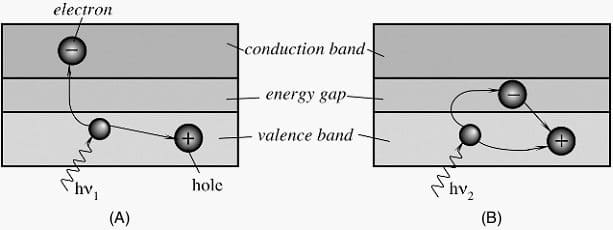
Figure 1A shows energy bands of a semiconductor material, where Eg is the magnitude in electron volts (eV) of the forbidden band gap.
The lower band is called the valence band, which corresponds to those electrons that are bound to specific lattice sites within the crystal. In the case of silicon or germanium, they are parts of the covalent bonding which constitute the interatomic forces within the crystal. The next higher-lying band is called the conduction band and represents electrons that are free to migrate through the crystal. Electrons in this band contribute to the electrical conductivity of the material.
The two bands are separated by the band gap, the size of which determines whether the material is classified as a semiconductor or an isolator.
The number of electrons within the crystal is just adequate to completely fill all avail-able sites within the valence band. In the absence of thermal excitation, both isolators and semiconductors would therefore have a configuration in which the valence band is completely full and the conduction band completely empty. Under these imaginable circumstances, neither would theoretically show any electrical conductivity.
Metals, therefore, are always characterized by a very high electrical conductivity. In isolators or semiconductors, on the other hand, the electron must first cross the energy band gap in order to reach the conduction band and the conductivity is, therefore, many orders of magnitude lower.
Table 1: Band Gaps and Longest Wavelengths for Various Semiconductors
| Material | Band Gap (eV) | Longest Wavelength (µm) |
| ZnS | 3.6 | 0.345 |
| CdS | 2.41 | 0.52 |
| CdSe | 1.8 | 0.69 |
| CdTe | 1.5 | 0.83 |
| Si | 1.12 | 1.10 |
| Ge | 0.67 | 1.85 |
| PbS | 0.37 | 3.35 |
| InAs | 0.35 | 3.54 |
| Te | 0.33 | 3.75 |
| PbTe | 0.30 | 4.13 |
| PbSe | 0.27 | 4.58 |
| InSb | 0.18 | 6.90 |
For isolators, the band gap is usually 5 eV or more, whereas for semiconductors, the gap is considerably less (Table 1). Note that the longer the wavelength (lower frequency of a photon), the less energy is required to originate a photoeffect.
When the photon of frequency υ1 strikes the crystal, its energy is high enough to separate the electron from its site in the valence band and push it through the band gap into a conduction band at a higher energy level. In that band, the electron is free to serve as a current carrier. The deficiency of an electron in the valence band creates a hole which also serves as a current carrier.
This is manifested in the reduction of specific resistivity of the material. On the other hand, Figure 1B shows that a photon of lower frequency υ2 does not have sufficient energy to push the electron through the band gap. The energy is released without creating current carriers. The energy gap serves as a threshold below which the material is not light sensitive.
However, the threshold is not abrupt. Throughout the photon-excitation process, the law of conservation of momentum applies.
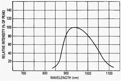
The momentum and density of hole-electron sites are higher at the center of both the valence and conduction bands, and they fall to zero at the upper and lower ends of the bands. Therefore, the probability of an excited valence-band electron finding a site of like momentum in the conduction band is greater at the center of the bands and is the lowest at the ends of the bands. Therefore, the response of a material to photon energy increases from Eg gradually to its maximum and then falls back to zero at the energy corresponding to the difference between the bottom of the valence band and the top of the conduction band.
A typical spectral response of a semiconductive material is shown in Figure 2.
The light response of a bulk material can be altered by adding various impurities. They can be used to reshape and shift a spectral response of the material. All devices that directly convert photons of electromagnetic radiation into charge carriers are called quantum detectors and are generally produced in a form of photodiodes, phototransistors, and photoresistors.
When comparing the characteristics of different photodetectors, the following specifications usually should be considered:
NEP (noise-equivalent power) is the amount of light equivalent to the intrinsic noise level of the detector. Stated differently, it is the light level required to obtain a signal-to-noise ratio equal to unity.
Because the noise level is proportional to the square root of the bandwidth, the NEP is expressed in units of W/√Hz:

D* refers to the detectivity of a detector’s sensitive area of 1 cm2 and a noise bandwidth of 1 Hz:

Detectivity is another way of measuring the sensor’s signal-to-noise ratio. Detectivity is not uniform over the spectral range for operating frequencies; therefore, the chopping frequency and the spectral content must be also specified. The detectivity is expressed in units of cm √Hz/W.
IR cutoff wavelength (λc) represents the long-wavelength limit of the spectral response and often is listed as the wavelength at which the detectivity drops by
10% of the peak value.
Maximum current is specified for photoconductive detectors (such as HgCdTe) which operate at constant currents. The operating current never should exceed the maximum limit.
Maximum reverse voltage is specified for Ge and Si photodiodes and photoconduc-tive cells. Exceeding this voltage can cause the breakdown and severe deteriora-tion of the sensor’s performance.
Radiant responsivityis the ratio of the output photocurrent (or output voltage) divided by the incident radiant power at a given wavelength, expressed in A/W or V/W.
Field of view (FOV) is the angular measure of the volume of space where the sensor can respond to the source of radiation.
Junction capacitance (Cj) is similar to the capacitance of a parallel-plate capacitor. It should be considered whenever a high-speed response is required. The value of Cj drops with reverse bias and is higher for the larger diode areas.


