Search

Premium Membership ♕

Save 50% on all EEP Academy courses with Enterprise Membership Plan and study specialized LV/MV/HV technical articles, guides and courses.

Home / Technical Articles / Power Semiconductor Device – Transistor
Power Semiconductor Device - Transistor
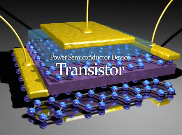
Power Semiconductor Device - Transistor (on photo: Tunnelling transistor based on vertical graphene heterostructures; credit: L. Britnel et al./Science)

Introduction

Power transistors are used in applications ranging from a few to several hundred kilowatts and switching frequencies up to about 10 kHz. Power transistors used in power conversion applications are generally npn type. The power transistor is turned on by supplying sufficient base current, and this base drive has to be maintained throughout its conduction period.

It is turned off by removing the base drive and making the base voltage slightly negative (within –VBE(max)).

The saturation voltage of the device is normally 0.5 to 2.5 V and increases as the current increases. Hence, the on-state losses increase more than proportionately with current. The transistor off-state losses are much lower than the on-state losses because the leakage current of the device is of the order of a few milliamperes.
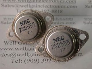
NEC 2SD555 NPN POWER TRANSISTOR VCB=400V 10A 200W TO-3

Because of relatively larger switching times, the switching loss significantly increases with switching frequency. Power transistors can block only forward voltages. The reverse peak voltage rating of these devices is as low as 5 to 10 V.

Power transistors do not have I2t withstand capability. In other words, they can absorb only very little energy before breakdown. Therefore, they cannot be protected by semiconductor fuses, and thus an electronic protection method has to be used. To eliminate high base current requirements, Darlington configurations are commonly used. They are available in monolithic or in isolated packages. The basic Darlington configuration is shown schematically in Figure 1.
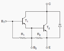
The Darlington configuration presents a specific advantage in that it can considerably increase the current switched by the transistor for a given base drive.
Figure-1 - A two-stage Darlington transistor with bypass diode.

The VCE(sat) for the Darlington is generally more than that of a single transistor of similar rating with corresponding increase in on-state power loss.

During switching, the reverse-biased collector junction may show hot-spot breakdown effects that are specified by reverse-bias safe operating area (RBSOA) and forward-bias safe operating area (FBSOA).

Modern devices with highly interdigited emitter base geometry force more uniform current distribution and therefore considerably improve secondary breakdown effects. Normally, a well-designed switching aid network constrains the device operation well within the SOAs.


Video Tutorials


SOURCE: Kaushik Rajashekara – Delphi Automotive Systems

Copyright Notice

This technical article is protected by U.S. and international copyright laws. Reproduction and distribution of PDF version of this technical article to websites such as Linkedin, Scribd, Facebook and others without written permission of the sponsor is illegal and strictly prohibited.

© EEP-Electrical Engineering Portal.

Premium Membership

Get access to premium HV/MV/LV technical articles, electrical engineering guides, research studies and much more! It helps you to shape up your technical skills in your everyday life as an electrical engineer.
More Information
Edvard Csanyi - Author at EEP-Electrical Engineering Portal

Edvard Csanyi

Hi, I'm an electrical engineer, programmer and founder of EEP - Electrical Engineering Portal. I worked twelve years at Schneider Electric in the position of technical support for low- and medium-voltage projects and the design of busbar trunking systems.

I'm highly specialized in the design of LV/MV switchgear and low-voltage, high-power busbar trunking (<6300A) in substations, commercial buildings and industry facilities. I'm also a professional in AutoCAD programming.

Profile: Edvard Csanyi

One Comment


  1. Jelena
    Oct 30, 2011

    Thank you Edvard on this article, very nice described.

Leave a Comment

Tell us what you're thinking. We care about your opinion! Please keep in mind that comments are moderated and rel="nofollow" is in use. So, please do not use a spammy keyword or a domain as your name, or it will be deleted. Let's have a professional and meaningful conversation instead. Thanks for dropping by!

  −  one  =  9

Learn How to Design Power Systems

Learn to design LV/MV/HV power systems through professional video courses. Lifetime access. Enjoy learning!

EEP Hand-Crafted Video Courses

Check more than a hundred hand-crafted video courses and learn from experienced engineers. Lifetime access included.
Experience matters. Premium membership gives you an opportunity to study specialized technical articles, online video courses, electrical engineering guides, and papers written by experienced electrical engineers.