The MCT is type of power semiconductor device that combines the capabilities of thyristor voltage and current with MOS gated turn-on and turn-off. It is a high power, high frequency, low conduction drop and a rugged device, which is more likely to be used in the future for medium and high power applications.
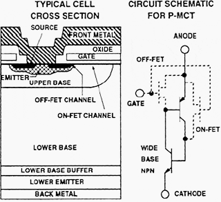
A cross-sectional structure of a p-type MCT with its circuit schematic is shown in Fig. 1.
The MCT has a thyristor type structure with three junctions and PNPN layers between the anode and cathode. In a practical MCT, about 100,000 cells similar to the one shown are paralleled to achieve the desired current rating.
MCT is turned on by a negative voltage pulse at the gate with respect to the anode, and is turned off by a positive voltage pulse.
The MCT was announced by the General Electric R & D Center on November 30, 1988.
Harris Semiconductor Corporation has developed two generations of p-MCTs. Gen-1 p-MCTs are available at 65 A/1000 V and 75A/600 V with peak controllable current of 120 A. Gen-2 p-MCTs are being developed at similar current and voltage ratings, with much improved turn-on capability and switching speed.
The reason for developing a p-MCT is the fact that the current density that can be turned off is 2 or 3 times higher than that of an n-MCT; but n-MCTs are the ones needed for many practical applications.
The advantage of an MCT over IGBT is its low forward voltage drop. N-type MCTs will be expected to have a similar forward voltage drop, but with an improved reverse bias safe operating area and switching speed. MCTs have relatively low switching times and storage time. The MCT is capable of high current densities and blocking voltages in both directions.
Since the power gain of an MCT is extremely high, it could be driven directly from logic gates. An MCT has high di/dt (of the order of 2500 A/μs) and high dv/dt (of the order of 20,000 V/μs) capability.
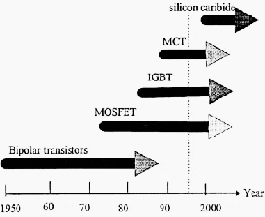
The current and future power semiconductor devices developmental direction is shown in Figure 2. High-temperature operation capability and low forward voltage drop operation can be obtained if silicon is replaced by silicon carbide material for producing power devices.

The silicon carbide has a higher band gap than silicon. Hence, higher breakdown voltage devices could be developed.
Silicon carbide devices have excellent switching characteristics and stable blocking voltages at higher temperatures. But the silicon carbide devices are still in the very early stages of development.
Resource: Mark Nelms – Auburn University


Thanks team,Articles posted is very useful to me,Really refreshing & Gaining additional knowledge!