
Estimated Study Time: 14 minutes
Basics about the subject
Various aspects of reactive power compensation problems have already been mentioned in previous articles. However, because of consistency of this article, we will remind ourselves briefly on basic terms and principles related to this field.
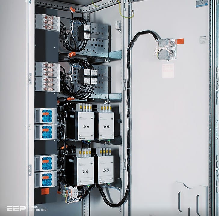 Why you should use advanced thyristor-switched reactive power compensation (photo credit: Janitza)
Reactive power is a sort of electrical power that circulates between inductances and capacitances inside the system. Unlike active power, reactive component does not transfer into useful energy, but it is necessary to exist, above all for the purpose of transformers and motors magnetization.
Since apparent (or total) power squared equals active power squared plus reactive power squared, we can easily conclude that for same amount of active power engaged, higher reactive power means that higher apparent power needs to be transferred. This further implies higher voltage drop values, and less line capacity for active power transmission in every part of electrical system loaded with reactive power.
Hence, it is our interest to compensate reactive power as near to reactive consumer as possible, and avoid the rest of lines and equipment upstream to be loaded with this sort of power.
Long power lines, because of their reactive (inductive and capacitive) nature, may also be used as reactive power source or consumer, depending on transmitted load value.
Thyristor, also known as SCR (Silicone Controlled Rectifier) is a component made of four semiconductor layers, which acts as semi-controlled bi-stable switch. There are three electrodes available on every thyristor: anode, cathode, and gate.
It is usually used for switching of main power circuit current between anode and cathode by use of small current impulse applied to the gate as trigger.
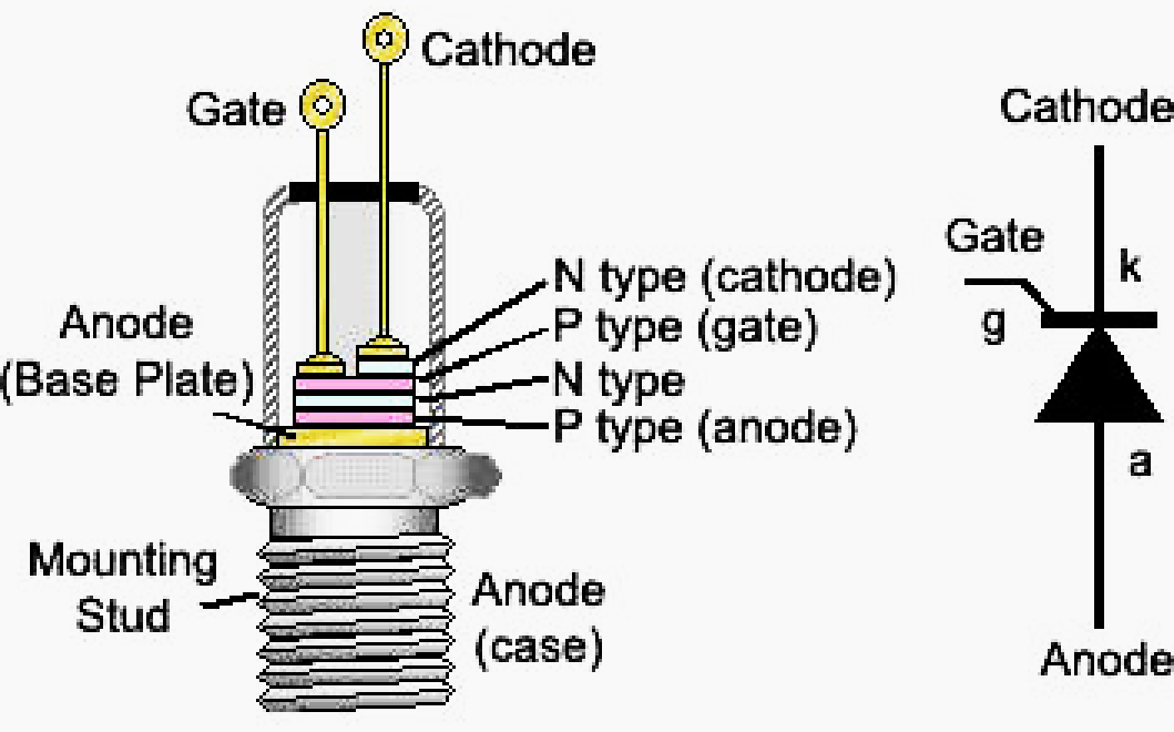
If thyristor is polarized directly, i.e. positively (anode potential is greater than cathode potential) it can be triggered into conducting state if current impulse is applied to the gate. Thyristor will remain conductive regardless to presence of gate impulse until current between anode and cathode falls below threshold called holding current. After that, positively polarized thyristor must be triggered by gate impulse again in order to conduct.
If thyristor is polarized inversely, i.e. negatively (anode potential is smaller than cathode potential) it cannot conduct, regardless of gate impulse presence.
Since effective (RMS) value of voltage on load side depends on portion of conducted sine wave, this anti parallel connection of two thyristors is often used for various RMS regulation, light source dimming for example.
Reactive power compensation using thyristors
When variable reactive load needs to be compensated, so called automatic compensation is applied. In most cases, it assumes installation of total required additional reactive power in the form of several groups of capacitors (with or without reactors), together with switching devices. Each group is connected in parallel with compensated load, and usually referred to as “compensation step”.
Switching devices are controlled by microprocessor based regulator, which is capable to switch on or off most suitable compensation step, according to real time consumption of reactive power and required displacement power factor.
Typical switching device for this purpose is three pole, mechanically operated contactor, designed for capacitive current switching. Each capacitor is equipped with discharging resistors.
Because of above explained reason, there is adjustable parameter of regulation, usually called “discharge time”, “switching on delay” or similar. During this period of time after disconnection, regulator will not connect the same step again, so that step will not be available for increase of reactive power, even if regulator calculates that it is the optimal choice for switching on.
In other words, regulator has to wait for capacitor voltage to drop at acceptable value, which will not cause harmful effect during connection to network. For typical solutions, this discharge time parameter is usually set to at least 30 seconds. So, we could say that this basic, discrete (stepwise) regulation technique is not quite flexible or responsive.
However, for majority of applications, this relatively cheap solution does the job successfully because:
Reason #1
In most cases, bulk (centralized) reactive power compensation is applied, with capacitors connected to main LV busbars inside MV/LV substation. At this point of installation, fluctuations of reactive power consumption usually aren’t very severe and frequent.
Reason #2
Mean value of displacement power factor, usually over one month period, is valid for electrical utility tariff system and monthly cost. From economical point of view, that further means that periods with lower power factor caused by lack of appropriate compensation power can be tolerated, because they will be compensated with periods during which power factor will be higher than required value.
In Figure 2, example of such switching device, called “thyristor switching module for power factor correction” is shown. These modules contain two thyristors in antiparallel connection within two of three phases (third phase is not switched).
Related electrical guides & articles


Miodrag Kokotovic
Graduated from Faculty of Electrical Engineering, within University of Belgrade, in the field of electrical power systems. Expert in electrical part of tender preparation, design, procurement, construction and commissioning of treatment plants and pumping stations, electrical power quality and energy management.Profile: Miodrag Kokotovic
